We have compiled a list of manufacturers, distributors, product information, reference prices, and rankings for Growth Equipment.
ipros is IPROS GMS IPROS One of the largest technical database sites in Japan that collects information on.

Growth Equipment Product List and Ranking from 5 Manufacturers, Suppliers and Companies | IPROS GMS

Last Updated: Aggregation Period:May 27, 2026~Jun 23, 2026
This ranking is based on the number of page views on our site.

Growth Equipment Manufacturer, Suppliers and Company Rankings

Last Updated: Aggregation Period:May 27, 2026~Jun 23, 2026
This ranking is based on the number of page views on our site.

  1. 三幸 Tokyo//Electronic Components and Semiconductors
  2. 北野精機 Tokyo//Manufacturing and processing contract
  3. ケニックス Hyogo//Electronic Components and Semiconductors
  4. 4 山口ティー・エル・オー Yamaguchi//Government
  5. 4 Global Reports Tokyo//others

Growth Equipment Product ranking

Last Updated: Aggregation Period:May 27, 2026~Jun 23, 2026
This ranking is based on the number of page views on our site.

  1. Crystal growth furnace using high-frequency induction heating method 三幸
  2. Carbon Nanotube Growth Device (KCNT) 北野精機
  3. SIC surface thermal decomposition method for graphene crystal growth apparatus ケニックス
  4. Semiconductor substrate and its manufacturing method, as well as a vapor phase growth apparatus used for it. 山口ティー・エル・オー
  5. 4 Global market size of silicon carbide epitaxial growth equipment. Global Reports

Growth Equipment Product List

1~5 item / All 5 items

Displayed results

Carbon Nanotube Growth Device (KCNT)

Carbon Nanotube Growth Device (KCNT)

●Features Carbon nanotubes come in many varieties due to differences in their outer diameter and structure, all made from carbon atoms that are strongly bonded together. Their unique structure gives them the following properties: - Excellent electrical conductivity. - Excellent thermal conductivity. - Excellent mechanical properties. This device uses an electric furnace to heat a substrate in a quartz tube up to 900°C, introducing ethanol gas to grow carbon nanotubes.

  • Analytical Equipment and Devices
  • Other laboratory equipment and containers
  • Growth Equipment

Added to bookmarks

Bookmarks list

Bookmark has been removed

Bookmarks list

You can't add any more bookmarks

By registering as a member, you can increase the number of bookmarks you can save and organize them with labels.

Free membership registration

SIC surface thermal decomposition method for graphene crystal growth apparatus

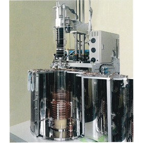
Equipped with a heating mechanism suitable for the growth of thermally decomposed graphene on SiC substrates.

The design and development concept of the epitaxial graphene crystal growth device using the sic surface thermal decomposition method focuses on miniaturization and simplification of the graphene growth apparatus. It aims for high crystal quality and reproducibility of growth, as well as the addition and connectivity of surface analysis equipment, making it economically feasible for investment. The formation of graphene was confirmed from the diffraction pattern. A graphene/buffer layer has been formed. The streaks are believed to be due to the one-dimensional structure of graphene on the facets. Graphene is uniformly formed on terraces (0001) approximately 250 nm wide, and the periodic structure is a result of step punching unique to the off-substrate. The formation of graphene was also confirmed through micro-Raman measurements. The Raman spectra of the terraces (red) and facets (blue) shown in the optical microscope image of the sample surface are presented. It is a typical graphene spectrum, confirming that it is a single layer graphene based on the half-width of the 2D peak. Additionally, the D band is significantly larger on the facets, which is believed to reflect the one-dimensional structure of graphene. This was clearly observed in the mapping as well. For more details, please contact us or refer to the catalog.

  • others
  • Growth Equipment

Added to bookmarks

Bookmarks list

Bookmark has been removed

Bookmarks list

You can't add any more bookmarks

By registering as a member, you can increase the number of bookmarks you can save and organize them with labels.

Free membership registration

Semiconductor substrate and its manufacturing method, as well as a vapor phase growth apparatus used for it.

Warping caused by differences in physical constants is canceled out between both surfaces! It is possible to manufacture semiconductor substrates with minimal warping!

The issue of warping in GaN substrates leads to high costs due to low yield, as well as low crystal quality and small areas of low quality, which in turn becomes the biggest factor hindering the widespread adoption of GaN substrates. The present invention aims to produce semiconductor substrates with minimal warping using a vapor phase growth method. By alternately growing semiconductor crystals on both sides of the base substrate using the vapor phase growth method, the warping caused by differences in physical constants such as the thermal expansion coefficients of the base substrate and the semiconductor is canceled out between the two sides, making it possible to manufacture semiconductor substrates with minimal warping. 【Key Solutions】 - Manufacturing semiconductor substrates by growing semiconductor crystals on the base substrate using the vapor phase growth method. - A process in which raw gas is brought into contact with one principal surface of the base substrate to grow semiconductor crystals on the base substrate. - Another process in which raw gas is brought into contact with the other principal surface of the base substrate to grow semiconductor crystals on the base substrate. - Alternating between the first process and the other process. *For more details, please refer to the PDF document or feel free to contact us.

  • Other semiconductors
  • Growth Equipment

Added to bookmarks

Bookmarks list

Bookmark has been removed

Bookmarks list

You can't add any more bookmarks

By registering as a member, you can increase the number of bookmarks you can save and organize them with labels.

Free membership registration

Crystal growth furnace using high-frequency induction heating method

Single crystal growth apparatus using the Cz method with high-frequency induction heating.

Our crystal growth furnace is designed based on the requirements for oxide single crystals, which include "high melting point, oxygen atmosphere, and long-term stable control." *For more details, please feel free to contact us at the information below.* Sankou Co., Ltd. Headquarters Sales Department TEL: 03-5403-9250

  • Electric furnace
  • Growth Equipment

Added to bookmarks

Bookmarks list

Bookmark has been removed

Bookmarks list

You can't add any more bookmarks

By registering as a member, you can increase the number of bookmarks you can save and organize them with labels.

Free membership registration

Global market size of silicon carbide epitaxial growth equipment.

This report systematically organizes the medium- to long-term growth trends of the silicon carbide epitaxial growth equipment market through both quantitative and qualitative analyses.

This document provides an explanation of the global market size for silicon carbide epitaxial growth equipment. It covers an overview of silicon carbide epitaxial growth equipment, analysis by product type, analysis by application, analysis by company, analysis by region, technological innovations, and future market outlook. Our company, based in Tokyo, integrates industrial information from around the world and provides reports to support corporate decision-making. *For more details, please download the PDF or feel free to contact us.*

  • others
  • Growth Equipment

Added to bookmarks

Bookmarks list

Bookmark has been removed

Bookmarks list

You can't add any more bookmarks

By registering as a member, you can increase the number of bookmarks you can save and organize them with labels.

Free membership registration